Whats The Difference PCB Routing Then and Now Circuit Diagram
Whats The Difference PCB Routing Then and Now Circuit Diagram The printed circuit board (PCB) routing problem has been studied extensively in recent years. Due to continually growing net/pin counts, extremely high pin density, and unique physical constraints, the manual routing of PCBs has become a time-consuming task to reach design closure.

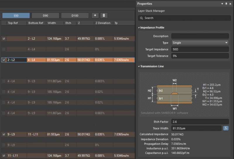
PCB routing is a critical aspect of electronic design that directly impacts the performance, manufacturability, and cost of electronic products. This comprehensive guide explores various routing strategies, best practices, and optimization techniques for creating efficient PCB layouts. Now, let's explore specific routing techniques that can help reduce the influence of EMI in high-speed PCB designs. 1. Layer Stack-up Optimization. Mastering high-speed PCB routing techniques for EMI reduction is crucial in today's electronic design landscape. By implementing the strategies outlined in this guide - from optimizing PCB Routing Optimization. Reasonable PCB routing is the key to reducing signal interference. It can effectively control signal impedance, delay, and crosstalk. Signal Line Routing Principles: Shortest Path: Signal lines should use the shortest path to reduce signal transmission distance and reduce signal attenuation and reflection.
Optimized Placement and Routing for PCB Design Circuit Diagram
Therefore, AI-based PCB insertion and routing automation methods have been developed. This research suggests using AI to optimize PCB component arrangement and routing. The system uses machine learning and optimization to improve design efficiency. The AI system creates layouts that match performance requirements, decrease signal interference PCB routing is an essential step in the design process that significantly impacts the performance and reliability of electronic devices. By following best practices such as proper trace width selection, effective ground and power plane usage, and controlled impedance routing, designers can ensure optimized signal flow and reduce the risk of
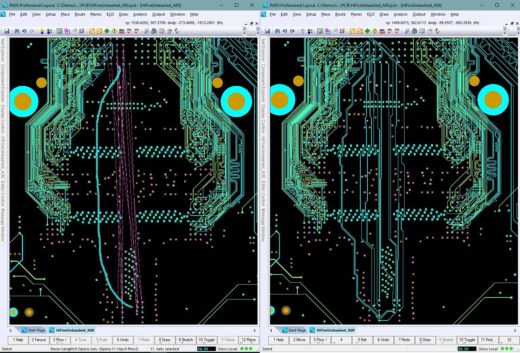
Complex PCB routing requires rules and constraints for success. As PCB designers, setting up rules and PCB design constraints for routing a printed circuit board is a critical part of our job. It can take time and involve research and manual input, but setting up these constraints and routing your board according to the rules can save your

RayMing PCB: Routing Strategy in PCB Layout Circuit Diagram
PCB routing is a complex yet essential aspect of circuit design that directly impacts the performance, reliability, and functionality of electronic devices. Mastering PCB routing techniques, from circuit design and trace optimization to high-speed routing and signal integrity, is crucial for creating efficient and reliable PCBs.